TPUs and Neural Engines
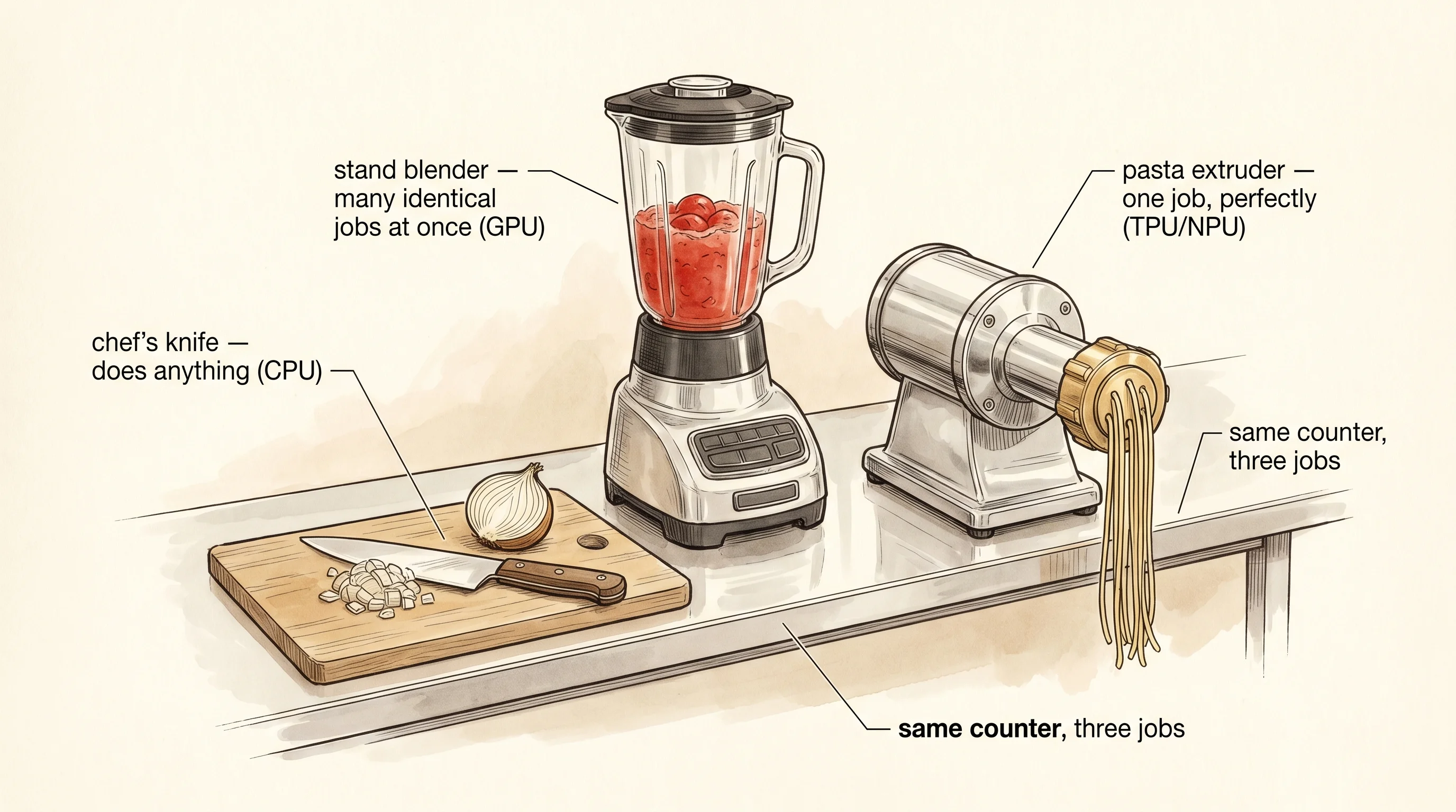
A home kitchen has one chef's knife and the chef uses it for everything — onions, chicken, herbs, bread. A restaurant kitchen has the same chef's knife and adds a stand blender to crush a thousand identical tomatoes for marinara, because a knife doing tomatoes one at a time would burn the night. A pasta factory has both and adds a thirty-thousand-dollar extruder that does exactly one thing — push dough through a brass die — and does it faster and quieter and with less electricity than any blender ever could. The chef's knife is the CPU. The stand blender is the GPU. The pasta extruder is the chip this lesson is about, and there is now one inside every iPhone and one stack of them in every Google data center.
The story starts with a panicked memo at Google in 2013. Jeff Dean's team had measured what would happen if every Android user spoke three minutes a day to the new voice search feature, and the answer was that Google would have to double the number of data centers it owned. The math underneath voice recognition was neural network math — millions of multiply-and-add operations stacked into matrices — and CPUs were doing it one number at a time. GPUs helped, but GPUs were built to draw triangles for video games, and most of their silicon was for things neural networks did not need. Norm Jouppi, a senior hardware engineer Google had just hired from HP, was given fifteen months to design a chip that did matrix math and nothing else. The first Tensor Processing Unit shipped in 2015 and was already running inside the data center before most of Google's own engineers knew it existed.
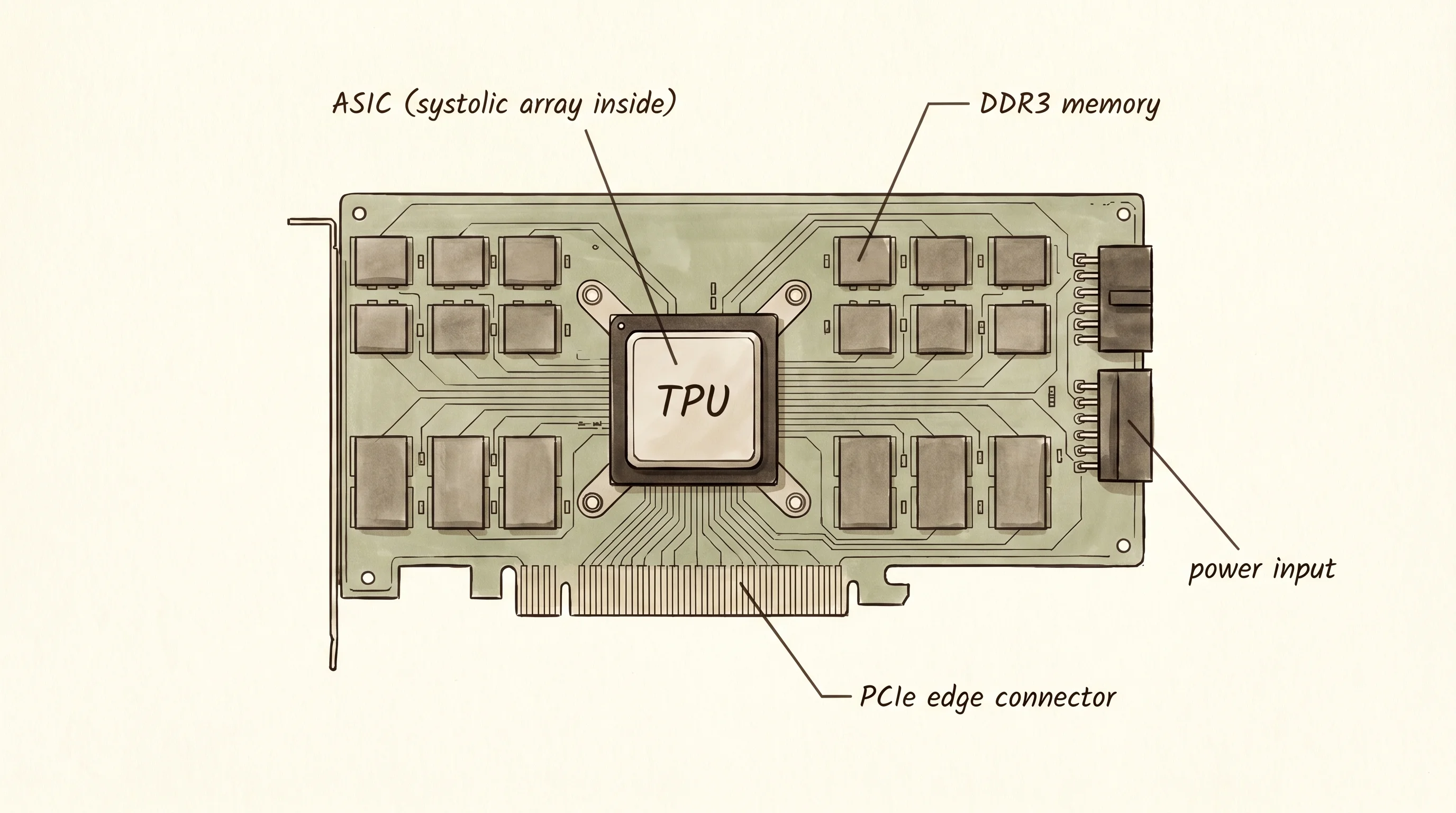
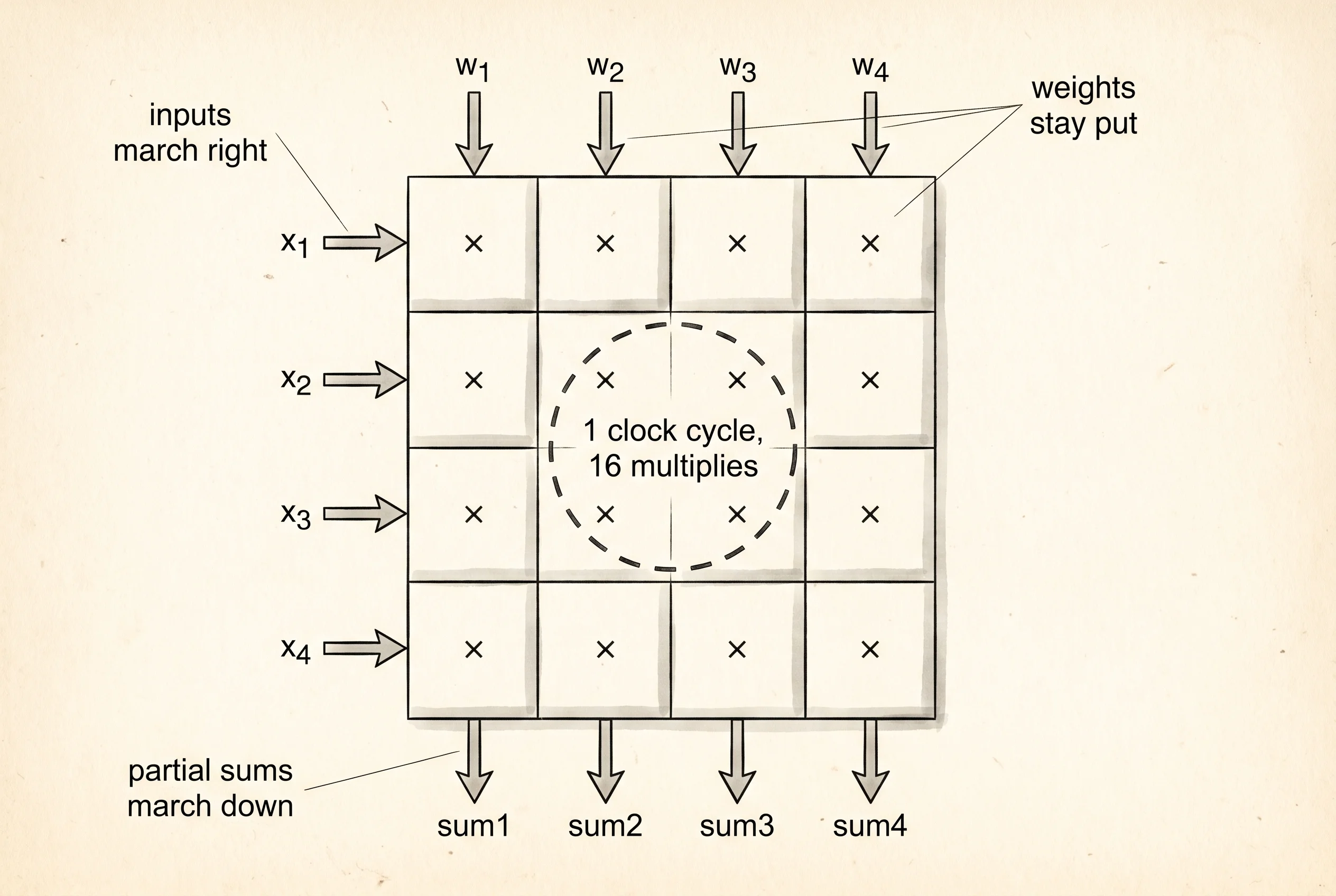
The trick Jouppi used was called a systolic array, an idea from a Carnegie Mellon professor named H. T. Kung who had published it in 1979. A systolic array is a grid of tiny multipliers wired so that numbers flow through them like blood through a heart — partial sums march downward while inputs march rightward, and after one pass through the grid an entire matrix multiplication has finished. A 256-by-256 systolic array does 65,536 multiplies per clock cycle. A CPU core, at its best, does one. The chip Jouppi's team built had no branch predictor, no out-of-order engine, no cache hierarchy, no support for any of the thousand instructions a normal CPU understands. It had the array and a few buffers around it. That was the whole chip, and that was the point.
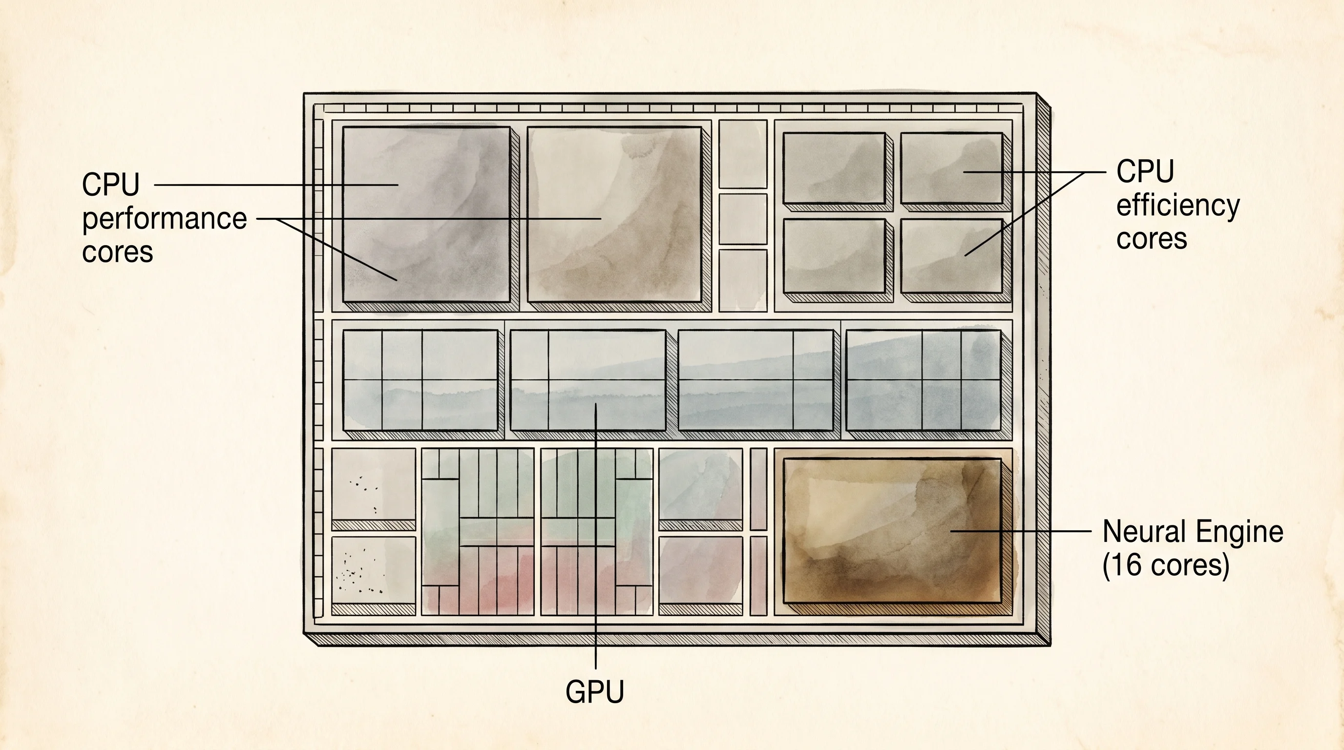
Apple was watching. The first iPhone shipped in 2007 ran every machine learning task on the CPU, which is why early Siri sent your voice to a data center to be transcribed — the phone could not do it fast enough or cheaply enough on battery. By 2017 Apple had its own answer. The iPhone X shipped with an A11 Bionic, and tucked into the corner of that chip was a two-core block Apple called the Neural Engine. It was the same idea as the TPU but shrunken to fit a phone — a few hundred multipliers wired to do convolutions and matrix math directly, with no general-purpose compute. The Neural Engine ran Face ID. Face ID needed to compare a three-dimensional scan of your face against a stored template in under a second, on battery, without ever phoning home. The CPU could not do it. The GPU could do it but would drain the battery. The Neural Engine did it in milliseconds, sipping less power than the screen.
Here is a small Rust program that puts the four chips of this story on one page. It lists each one, what it is built for, its peak speed in trillions of operations per second, and how many watts it burns to hit that speed. The last column is what matters — operations per watt, the only number a phone designer cares about and the only number a data center accountant cares about.
struct Chip {
    name: &'static str,
    job: &'static str,
    peak_tops: f32,
    watts: u32,
}

const CHIPS: &[Chip] = &[
    Chip {
        name: "Intel i9 CPU",
        job: "anything, one thing at a time",
        peak_tops: 1.0,
        watts: 125,
    },
    Chip {
        name: "NVIDIA RTX 4090 GPU",
        job: "thousands of identical math ops",
        peak_tops: 660.0,
        watts: 450,
    },
    Chip {
        name: "Google TPU v5p",
        job: "matrix multiply, nothing else",
        peak_tops: 918.0,
        watts: 192,
    },
    Chip {
        name: "Apple M3 Neural Engine",
        job: "on-device inference",
        peak_tops: 18.0,
        watts: 8,
    },
];
fn main() {
println!("four chips, four jobs");
println!(
"{:<24} {:<35} {:>10} {:>7} {:>11}",
"chip", "what it is built for", "peak TOPS", "watts", "TOPS/watt",
);
println!("{}", "-".repeat(92));
for c in CHIPS {
let per_watt = c.peak_tops / c.watts as f32;
println!(
"{:<24} {:<35} {:>10.1} {:>7} {:>11.3}",
c.name, c.job, c.peak_tops, c.watts, per_watt,
);
}
println!("{}", "-".repeat(92));
println!();
println!("the ASIC tax: how many cycles a 4x4 matmul takes");
println!(" CPU scalar loop ........... 64 multiplies, one at a time");
println!(" GPU SIMD lane ............. 16 multiplies per clock, four clocks");
println!(" TPU systolic array ........ one clock, the whole matrix at once");
println!(" NPU fused multiply-add .... one clock, then sleep");
}Compile it and run it.
four chips, four jobs
chip                     what it is built for                 peak TOPS   watts   TOPS/watt
--------------------------------------------------------------------------------------------
Intel i9 CPU             anything, one thing at a time              1.0     125       0.008
NVIDIA RTX 4090 GPU      thousands of identical math ops          660.0     450       1.467
Google TPU v5p           matrix multiply, nothing else            918.0     192       4.781
Apple M3 Neural Engine   on-device inference                       18.0       8       2.250
--------------------------------------------------------------------------------------------

the ASIC tax: how many cycles a 4x4 matmul takes
  CPU scalar loop ........... 64 multiplies, one at a time
  GPU SIMD lane ............. 16 multiplies per clock, four clocks
  TPU systolic array ........ one clock, the whole matrix at once
  NPU fused multiply-add .... one clock, then sleep
Read the last column. The TPU does five hundred and ninety times more math per watt than an Intel CPU. The Neural Engine does two hundred and eighty times more. Numbers that big are not refinements — they are the reason an entirely different chip exists. Every time you ask Siri something, every time the Photos app finds your dog in a five-year-old picture, every time Google Translate runs on your phone with no signal, the work is happening on silicon that cannot do anything else and would be useless for any task you would ever write in C. The bottom block of the output is the why: a 4-by-4 matrix multiply takes a CPU 64 separate operations, takes a GPU 4 clock ticks, and takes a TPU exactly one tick because the whole matrix lives in the grid at once. The specialized chip wins because it threw away every feature it did not need.
Here is what bites a Rust programmer trying to use one of these chips. Neither the TPU nor the Neural Engine speaks an instruction set you can target with rustc. There is no --target=tpu-v5p flag. The chip lives behind a runtime — Google's XLA compiler for TPUs, Apple's Core ML framework for the Neural Engine — and that runtime only knows how to accept a graph of tensor operations from a higher-level framework. The graph gets compiled down to the chip's private firmware language and shipped to the silicon. Your Rust code talks to that runtime through a binding crate, usually tch for PyTorch or candle for a pure-Rust path, and what you hand the binding is a description of the math, not the math itself. The chip never sees your loop. The chip sees a compiled blob the runtime built for it.
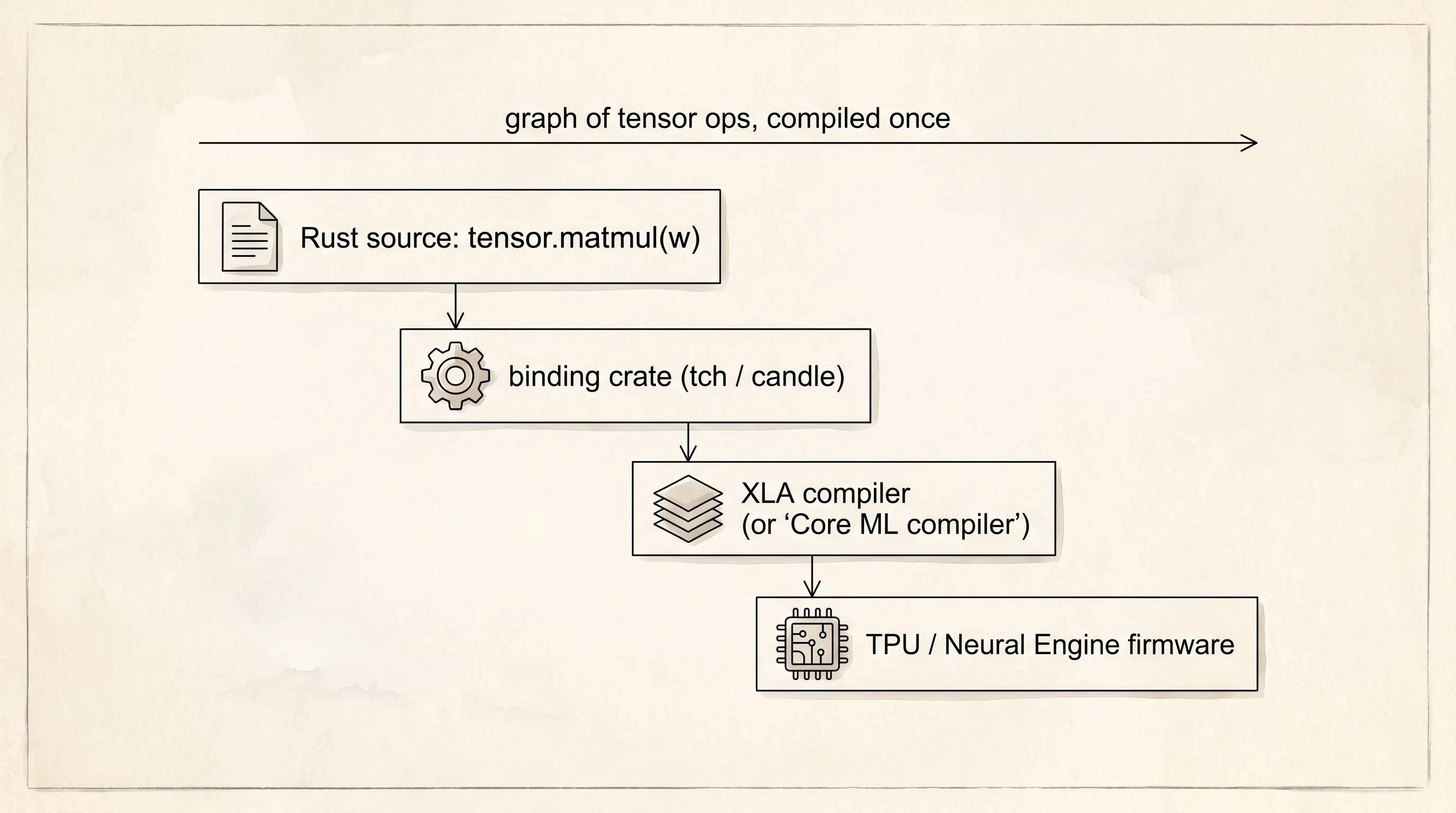
That indirection is the price of the speed. A CPU runs whatever you give it because it was built to run anything. A TPU runs only what the runtime knows how to compile because the chip has no general-purpose front end to fall back on. If your model uses an operation Core ML cannot lower, the Neural Engine sits idle and the CPU does that part. The win is enormous when the graph fits, and zero when it does not.
The next bottleneck is that everything in this section has been the silicon side of the story — the boxes the bits move through; the next section opens up the kernel that decides which program gets to use that silicon and when.